
The most-awaited convergence of microelectronics and photonics promises to bring about a revolution for on-chip data communications and processing. Among all the optoelectronic devices to be developed, power-efficient nanolaser diodes able to be integrated densely with silicon photonics and electronics are essential to convert electrical data into the optical domain.
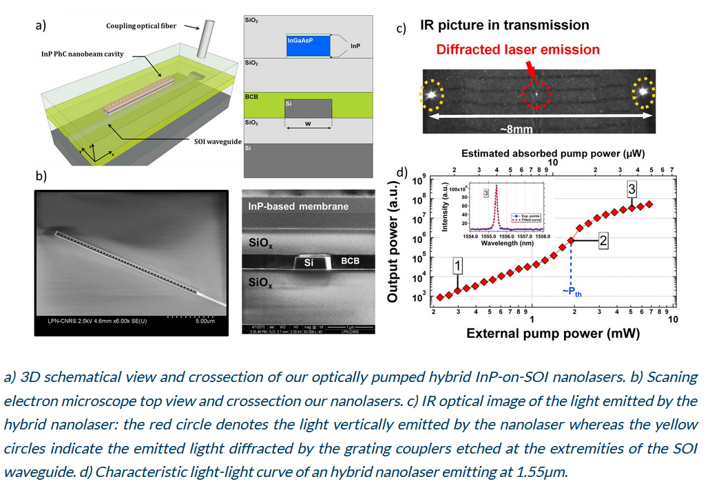
In our team, we have identified photonic crystals nanocavities to be the best suited candidates for low thresholds or even thresholdless laser operation with ultrafast dynamics. Indeed, these structures provide tight localization of the electromagnetic field enabling enhanced light–matter interaction and the control of spontaneous emission. More precisely, we have been working on hybrid structures comprising an InP-based photonic crystal nanocavity positioned on top of a silicon on insulator waveguide (see Figure below a) and b)) to allow evanescent wave coupling.
However, electrically driven stable room temperature CW lasing with output powers beyond a few microwatts remains a challenge, as several hurdles have to be overcome simultaneously: nanometre-precise material processing, poor heat sinking, large non-radiative surface recombination of carriers, complex optical interfacing and electrical injection.
Our goal is to propose innovative approaches to solve each and everyone of these issues and to explore novel concept of nanolasers taking advantage of the versatility of the hybrid configuration.